
Simplified diagram
Background
University of Electro-Communications Research Laboratories is conducting research on optical sensors and devices utilizing unique MEMS structures, such as micro-nano-size diffraction gratings, pillar structures, or stereo-helical structures.
We are working to design and develop optical sensors such as optical sensors and optical filters using this MEMS technology. Also we are working on silicon to develop optical elements which has the nano dimensions of micro-micrometer and nanometer. If the material is silicon, the current manufacturing process of semiconductor can be used. This means that we can mass-produce the optical element for such a low price. Specifically, we expect to develop ultra-small spectrometers, high-performance infrared sensors, or polarization filters for far-infrared light etc. In this article especially, we introduce ultra-small spectrometer. Spectroscopic and spectral cameras (spectral information in wide-spectrum cameras, such as hyper multispectral cameras, multispectral cameras, etc.) are widely used in industrial fields. Based on our technology of the principle of MEMS mechanisms, we are doing a research about spectral means that is very small, the simple manufacturing process and cost-effective. We welcome anyone who is interested in realizing its practical use and joint research of this technology with us.
Technical Content
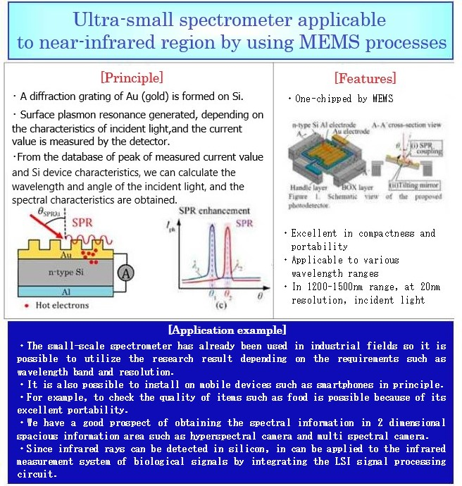
In this study, Au (gold) is deposited on Si (silicon) surfaces, and the diffraction grating is formed by an uneven structure on Au. The formation of this grating is done by the MEMS process. Depending on the condition of the incident angle and the wavelength of the light when the light hits, the resonance is generated by the surface plasmon phenomenon, and the current generated by the resonance is measured by the detector.
Detecting surface plasmon by diffraction grating
■Resonance of surface plasmon (SPR)
■Resonance of free electron generated by Au and inductor interface (air)
■Excitation by lighting Au diffraction grating
■Resonance of special conditions (angle of lighting, wavelength of light)
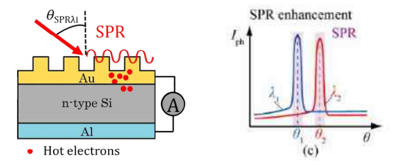
By making the grating on semiconductor, it is possible to detect the resonance by electric current.
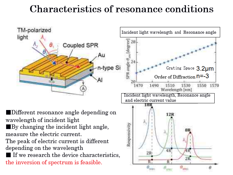
The peak of the current value detected by the detector is determined by the wavelength and the light angle, and the characteristics of the device (Si).
On the contrary, if we know the characteristics of the device and the peak of the current value when the light is irradiated, the wavelength and angle of the incident light are derived from the inverse matrix (inverse of the spectrum).
Strengths of the Technology and Know-How (Novelty, Superiority, Utility)
The conventional small-scale spectrometer detects light separated by a grating by a photodetector. Therefore, there is a limit to miniaturization because the optical path length is necessary to disperse the light. This technology solved the problem by using a detector to measure the current value and is integrated as a device. Also, we realized one-chipped incorporated actuator to operate the incident angle (On research about the way of controlling incident light angle as well as MEMS actuator).
The several mm of thickness and about 1 cm wide spectrometer has some good prospect of realizing in service.
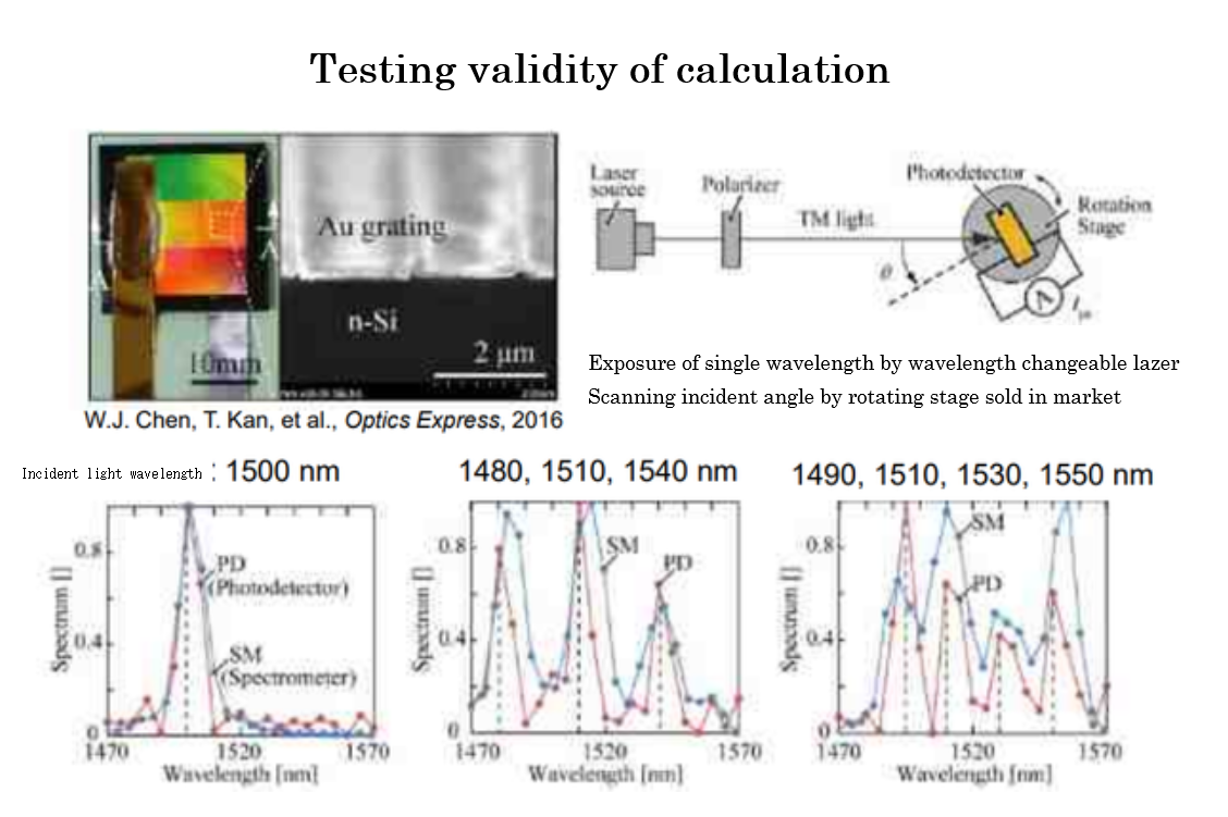
This technology uses MEMS process to create devices, but it is a common technique that is widely used in industry as its process. Therefore, it is low cost and mass-production processes is not so difficult. The validity of the measurement accuracy of the spectrometer on this technique is verified by using the scanning mechanism of the incident angle by the tunable laser and the rotating stage.
Committing to miniaturisation of MEMS
One-chipped MEMS
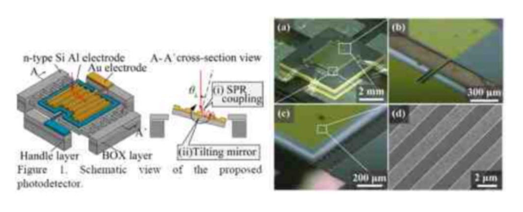
■Scanning angle feature installed
MEMS actuator
■Feasibility of thickness few mm and length 1cm spectrometer
As applicable wavelength range, a resolution of 20 nm is realized in the near-infrared region of 1200 nm to 1500 nm, for example. Resolution may be further improved. We also consider the realization of a spectrometer in the longer wavelength region and in the shorter wavelength region, such as in the infrared region and in the visible light region.
mage of Collaborative Companies
We welcome anyone who is interested in realizing its practical use and joint research of this technology. For example, we can cooperate with companies such as below.
1) The companies that are interested in developing new products and doing research and development using MEMS processes, etc.
2) The companies that are interested in developing products and use of this technology, and doing the development and sale of spectrometers, hyperspectral cameras, etc.
3) The companies and research institutes with the needs to utilize the spectrometer.
4) The companies that are interested in the use of this research object.
Utilization of Technologies and Know-How (Images)
・ Since it is small, it is also possible to install it on portable devices such as smartphones.
Its portability is excellent. You can even check the quality of your personal belongings, such as food quality.
・ It is also possible to obtain spectrum information for 2 dimensional space information areas such as hyperspectral cameras and multispectral cameras.
・ Since infrared rays can be detected by silicon, it can be applied to infrared measurement systems of biological signals by integrating LSI signal processing circuits.
Flow of Technology and Know-How Application
After your inquiry, we will introduce some detailed description of this technology and the prototypes. We can also respond to technical consultation related to MEMS processes. Please feel free to ask us.
Description of the Technical Terms
[Surface Plasmon Resonance]
Surface plasmon resonance (SPR) is a collective oscillation of free electrons induced by incident light. The resonance condition is achieved when the frequency of the photon (photons) is consistent with the natural frequency of the surface electrons of the positive charge.